When a PCB design is completed, the process is not over yet. In order for the design to be produced, the correct files must be sent to the manufacturer. At this point, one of the most frequently heard concepts in the electronic design world is the Gerber file.
PCB manufacturers do not directly use the design program's file to physically produce the board. Instead, they require standardized production files that define each layer of the board and its manufacturing details. Incorrect or incomplete production files can result in production delays, cost overruns and even completely faulty PCB production. In this article, we take a detailed look at what a Gerber file is, why it is critical in PCB manufacturing and which files should be prepared when sending to production.
What is the Gerber File?
The Gerber file is the standard production file format used in PCB manufacturing. It transfers copper paths, solder masks, text and other layer information on the board to the manufacturer. In short, the Gerber file is the PCB design translated into a language that the production machine can understand. PCB manufacturers determine how the board will be produced by looking at these files. The dimensions of the board, copper layers, solder mask openings and print layers are included in Gerber files. Today, the Gerber RS-274X format is used as the industry standard.
Is the Gerber File a Single File?
One of the most common mistakes beginners make is to think that Gerber is a single file. In fact, a PCB manufacturing package usually consists of multiple Gerber files.
For example:
- Top Copper (top copper layer)
- Bottom Copper (bottom copper layer)
- Top Solder Mask
- Bottom Solder Mask
- Silkscreen (print layer)
- Board Outline (board boundaries)
Each layer is created as a separate Gerber file and the manufacturer assembles these files together to produce the PCB. Therefore, missing layer exports are one of the most common causes of production errors.
Which Files are Required for PCB Production?
Many designers think that sending only Gerber files is enough. But professional production processes often require additional files.
A standard PCB production package consists of:
- Gerber files
- Drill File
- Pick and Place File
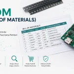
- BOM (Bill of Materials)
- Assembly Drawing
Especially if PCB typesetting service is to be received, only Gerber files are not sufficient. Component layout and assembly information must also be submitted to the manufacturer.
What is Drill File?
Holes on the PCB are not only defined with Gerber files. A separate Drill File is created for this process.
Drill is in the net:
- Via holes
- Mounting holes
- Through-hole contains all hole information such as component holes.
The PCB manufacturer performs drilling operations according to this file. Missing or incorrect drill file can cause serious problems in the production process. Especially in multilayer boards, the accuracy of hole coordinates is critical.
What is a Pick and Place File?
PCB production and PCB assembly are different processes. After the board is produced, a Pick and Place file is needed for SMT typesetters to place the components in the right spots.
For each component in this file:
- Reference number
- X-Y coordinate
- Rotation angle
- Layer information is available.
SMT machines use this data to automatically place components. Especially in high-volume production, even a small error in the Pick and Place file can affect the entire production.
Most Common Mistakes When Buying Gerber Export
A significant portion of the problems experienced in PCB production are caused by mistakes made during the export phase.
The most common problems are the following:
Exporting the wrong layers, missing board outline information, not creating a drill file and mismatches in units of measure can directly affect the production process. In addition, some designers send files without checking the Gerber Viewer before production. This may cause overlooked errors to be reflected in production. For this reason, it is strongly recommended to verify all files after export.
How to get Gerber on Altium, KiCad and Eagle
The basic logic is the same regardless of the PCB design program used. After the design is completed, production outputs are created and Gerber export is done by selecting the required layers. Then a drill file is created and all production files are prepared as a single package. Popular PCB design tools such as Altium Designer, KiCad and Autodesk Eagle all support the Gerber RS-274X format. However, since the export screen of each software is different, the files created must be checked before production.
The Role of the Gerber File in the PCB Typesetting Process
While Gerber files are critical for PCB production, they alone are not sufficient to complete the electronic board.
After the PCB is produced, SMT typesetting, soldering and testing processes begin. Pick and Place files, BOM lists and assembly drawings come into play at these stages.
Providing the production partner with a complete data package therefore not only reduces production time but also reduces the risk of errors.
File management is especially important in projects that transition from prototype to mass production.
Conclusion
Gerber files form the basis of PCB manufacturing and serve as technical documents that tell the manufacturer how to produce the board. However, Gerber files alone are not enough for a successful manufacturing process.
A complete production package with Drill file, Pick and Place file, BOM and assembly information should be prepared. Correctly exported files speed up the production process, while missing or incorrect files can cause cost and time loss.
As Elektroent, we provide support in all production preparation stages from Gerber control to BOM verification in PCB production and electronic card assembly processes, and help projects to be transferred to production smoothly.
If you want to get detailed information about the preparation of PCB production files for your project or electronic board typesetting processes, you can contact us.
+90 (216) 466 46 37