

The quality of electronics production depends to a large extent on how the board is assembled. The most widely used method in the world today SMD typesetting (Surface Mount Device - Surface Mount Technology) has become the cornerstone of modern electronics. In this article, we will explain what SMD board typesetting is, what stages it goes through and the critical points that directly affect your production decisions.
What is SMD Stringing?
SMD board assembly is the process of soldering electronic elements to the surface of a circuit board (PCB). Unlike the traditional through-hole mounting (THT) method, in SMD the elements do not pass through the board; they stick directly to the surface. This makes it possible to produce much smaller, lighter and higher density circuits.
From smartphones to automotive electronics, medical devices to industrial control panels, almost every modern electronic product uses SMD board array technology.
What is the SMD Typesetting Process?
1. PCB Preparation and DFM Inspection
Before the layout process starts, the circuit board design is examined for manufacturability (DFM - Design for Manufacturability). Pad dimensions, antenna spacing, thermal management zones are checked at this stage. Entering production with a faulty design leads to both cost and time loss.
2. Solder Paste Application (Stencil Printing)
Using a specially prepared stencil, solder paste is applied to the relevant areas of the circuit board. This step directly determines the quality of the subsequent soldering. Too much or too little paste and errors such as bridging or cold soldering are inevitable.
3. Pick & Place (Placement of Elements)
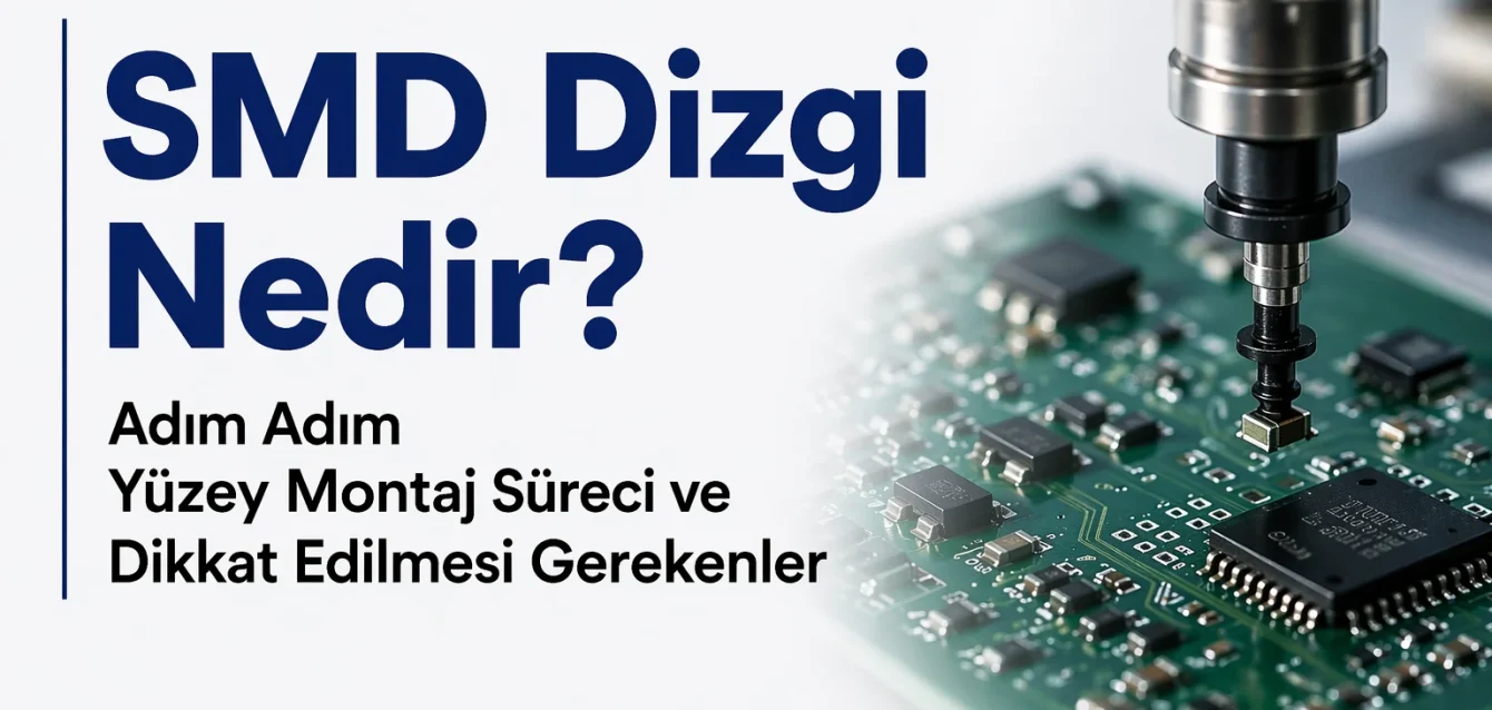
Automatic pick & place machines pick elements from roll or tray feeders and place them in the correct positions on the board with millimeter precision. High-speed machines can place tens of thousands of elements per hour.
4. Reflow Oven (Reflow Soldering)
After the elements are placed, the board is passed through a reflow oven with a controlled temperature profile. The heat curve inside the oven consists of four zones: preheat, activation, reflow and cool down. This profile ensures that the solder flows correctly and that the elements are not subjected to thermal stress.
5. Optical Inspection (AOI)
At the oven exit, the boards are passed through the Automatic Optical Inspection (AOI) system. AOI detects defects such as missing elements, wrong polarity, bridged solder points with cameras. Micro-level defects that the human eye might miss are caught early.
6. Double-sided Card Typesetting (If required)
If the board is double-sided, the same process is repeated for the second side of the board. The second side may require the use of adhesives or optimization of the oven profile to prevent the elements from falling against gravity.
7. Hand Soldering and After
Some elements (large connectors, special heatsinks, etc.) are soldered by hand by experienced technicians as they are not amenable to automation. The process is completed with electrical testing and functional verification.
Most Common Mistakes in SMD Stringing
The vast majority of disruptions in the production process are caused by a few basic reasons:
Cold Soldering Caused by insufficient heat or dirty pad surfaces. The board appears to be working but disconnects during vibration or temperature cycles.
Bridging: An unwanted solder bridge connecting two different pins. Especially common in ICs (integrated circuits) with narrow spacing.
Tombstoning: In small passive elements, one lead flows before the other and the element moves to a vertical position. It is directly related to the stencil design and the amount of solder paste.
Wrong Polarity Reverse placement of diodes or electrolytic capacitors. Although the AOI detects this error, it is essential that the routing signals are clear in the design phase.
Factors Determining Quality in SMD Card Typesetting
Just having the right machine is not enough. A quality SMD card typesetting service should include all of the following elements:
- Certified production environment: Compliance with IPC standards is a key indicator of production reliability.
- Choosing the right solder paste: Leaded (Sn63/Pb37) and lead-free (SAC305) pastes require different furnace profiles.
- Material tracking: Roll and tray based element tracking prevents the use of wrong elements during production.
- Test infrastructure: ICT (In-Circuit Test) or flying probe tests catch functional faults before mass production.
SMD Array or THT Array?
“Mixed array” projects using both technologies are becoming increasingly common. THT is preferred in high-current applications such as power electronics, while SMD is dominant in signal processing and control circuits. Choosing the right technology for your project's requirements is critical for both cost and long-term reliability.
Conclusion
When done right, SMD board typesetting offers the advantages of high production speed, low defect rate and compact design. However, each stage of the process - from design to oven, from inspection to testing - directly affects each other. Therefore, it is important to pay attention not only to price but also to infrastructure, certification and technical competence.